In this lecture we will think about the electronic behavior of solids. Why is carbon and insulator? Why is aluminum a conductor? What is the physics behind silicon electronics?
 Here is the same figure for 41 wells
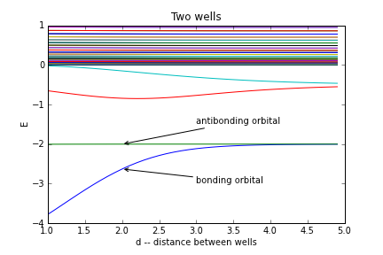
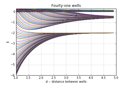 At any fixed distance it looks like there are ranges of energy for which you have a bunch of states, and ranges where you have no states. The former are called ``bands" while the latter are ``bandgaps" or simply ``gaps." A real crystal has $10^{23}$ wells, so these bands are pretty dense.
An insulator is a material where the Fermi energy is inside the gap. If you apply a voltage accross your insulator at $T=0$, you will get no current until the voltage is of order the band gap. There are simply no low energy states for the electrons. At finite temperature some of the electrons are thermally excited to the empty band, and they are able to carry current. The effective $n$ in our equation for conductivity, however, is very low. Thus, unless the temperature is of order the band gap, an insulator is a good insulator (even if it is a pure crystal).
An insulator with a small bandgap is known as a "semiconductor". Thus diamond, with a bandgap of 5eV is classified as an insulator, while silicon, with a bandgap of 1eV is a semiconductor. These energy scales make sense, since this is a typical atomic excitation energy -- and the bands are made up of the atomic levels.
Given that an eV corresponds to 10,000K, 1eV doesn't sound like it makes much of a difference at room temperature. A more important distinction is that a semiconductor is an insulator which is easily doped chemically. This means that you can tweak its composition a bit, and move the fermi energy into the band. By precisely tuning the composition, you can precisely tune the carrier density (which will roughly scale with the density of dopants). Closely related to doping is ``gating" where you apply potentials to move the Fermi energy around.
A conductor has the Fermi energy inside a band. The carrier density should be on the order of the density of lattice atoms.
At any fixed distance it looks like there are ranges of energy for which you have a bunch of states, and ranges where you have no states. The former are called ``bands" while the latter are ``bandgaps" or simply ``gaps." A real crystal has $10^{23}$ wells, so these bands are pretty dense.
An insulator is a material where the Fermi energy is inside the gap. If you apply a voltage accross your insulator at $T=0$, you will get no current until the voltage is of order the band gap. There are simply no low energy states for the electrons. At finite temperature some of the electrons are thermally excited to the empty band, and they are able to carry current. The effective $n$ in our equation for conductivity, however, is very low. Thus, unless the temperature is of order the band gap, an insulator is a good insulator (even if it is a pure crystal).
An insulator with a small bandgap is known as a "semiconductor". Thus diamond, with a bandgap of 5eV is classified as an insulator, while silicon, with a bandgap of 1eV is a semiconductor. These energy scales make sense, since this is a typical atomic excitation energy -- and the bands are made up of the atomic levels.
Given that an eV corresponds to 10,000K, 1eV doesn't sound like it makes much of a difference at room temperature. A more important distinction is that a semiconductor is an insulator which is easily doped chemically. This means that you can tweak its composition a bit, and move the fermi energy into the band. By precisely tuning the composition, you can precisely tune the carrier density (which will roughly scale with the density of dopants). Closely related to doping is ``gating" where you apply potentials to move the Fermi energy around.
A conductor has the Fermi energy inside a band. The carrier density should be on the order of the density of lattice atoms.
 There is no conductivity, since by the Pauli principle there are no places for the electrons to go.
On the other hand, if we get rid of one electron, there is now a "hole"
There is no conductivity, since by the Pauli principle there are no places for the electrons to go.
On the other hand, if we get rid of one electron, there is now a "hole"
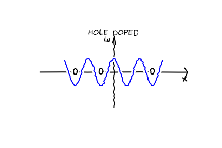 When a neighboring electron "hops" into the empty space, the hole moves around. To all external appearances it looks like the conductivity is due to the motion of these "positively charged holes." [For example, in the homework you will study the "Hall effect" which measures the charge of the carriers, and indeed finds positively charged carriers in "p-type" materials."
Thus we have two types of conductors.
When a neighboring electron "hops" into the empty space, the hole moves around. To all external appearances it looks like the conductivity is due to the motion of these "positively charged holes." [For example, in the homework you will study the "Hall effect" which measures the charge of the carriers, and indeed finds positively charged carriers in "p-type" materials."
Thus we have two types of conductors.
Drude model of conductivity
It turns out that the electronic properties of materials are completely quantum mechanical. Before discussing the quantum mechanics, however, we first need some language for discussing those properties. Hence we will begin with a simple classical model of conductivity. The basic physics of resistance is that electrons are slowed down when they bounce off of defects in a material. These could be lattice defects (like missing atoms or an atom in the wrong place) or they could be foreign impurities. A perfect three dimensional crystal with no impurities will it will either have a zero resistance -- like a perfect crystal of sodium, or an infinite resistance -- like a perfect crystal of diamond. Recall that you find resistance $R$ by dividing voltage by current. It is a device property, and has units of Volts per Amp (or equivalently, Ohms). If you make a resistor twice as long, the resistance should double (this is just resistors in series). If you double the cross-sectional area of a resistor, the resistance should fall by a factor of two (this is resistors in parallel). This scaling relation means that it makes sense to define a material parameter called resistivity $\rho$, defined so that \begin{equation} R=\frac{\rho L}{A} \end{equation} where $L$ is the length of our sample, and $A$ the cross-sectional area. Clearly $\rho$ has units of Volt-meters/Amp. On a microscopic scale, the current $I$ passing through our resistor can be thought of as distributed uniformly throughout each cross-section. It therefore makes sense to talk about a current density $j=I/A$. Similarly, the voltage drop across our resistor should be uniform, and it makes sense to talk of the voltage drop per unit length $E=V/L$. As the symbol suggests, this is just the electric field. The microscopic form of Ohm's law is \begin{equation} \rho=\frac{E}{j}. \end{equation} From a causal point of view, it is really the electric field that generates the current, so it is more natural to write this as \begin{equation} j=\frac{1}{\rho} E. \end{equation} This is so convenient of a way to thing about things that we define the conductivity $\sigma=1/\rho$. As an aside, the current density has a simple physical meaning. Current is the amount of charge per unit time flowing through our device. Thus current density is the amount of charge per unit time flowing through a unit area. Thus we expect \begin{equation} j=q n \bar v \end{equation} where $q$ is the carrier charge, $n$ is the carrier density, and $\bar v$ is the average speed So how do impurities influence the conductivity? The starting point is that an electron in a uniform electric field accelerates: \begin{equation} v(t)=v(0)+\frac{q E t}{m}. \end{equation} In the absence of impurities it will keep accelerating forever. When it hits an impurity, however, it gets scattered in a random direction, and the velocity "resets." Suppose it typically hits an impurity in a time $\tau$, known as the "mean-free-time." Its average speed will be \begin{equation} \bar v =\frac{1}{\tau} \int_0^\tau v(t)\,dt=v(0)+\frac{q E \tau}{2m}. \end{equation} We now average over all of the possible initial speeds, \begin{equation} \langle \bar v\rangle =\langle v(0)\rangle+\frac{q E \tau}{2m}. \end{equation} By symmetry $\langle v(0)\rangle=0$ and the average speed is $\bar v=q E \tau/2m$. The charge current is therefore \begin{equation} j=\frac{q^2 n\tau}{2m} E, \end{equation} from which we can read off the conductivity $\sigma=q^2 n\tau/2m$. [I would not be surprised if some authors absorb the factor of 2 into $\tau$.] There are three relevant things -- the density of electrons, the time between collisions, and the kinematic mass of the electrons. The distinction between a conductor and an insulator is predominantly the density of carriers. An insulator is one where $n\to 0$ as $T\to0$, and a conductor is one where $n$ is finite as $T\to 0$. When I say $n\to0$ I don't mean there are no electrons, rather I mean that the electrons are all bound to the nuclei, and do not move around. The other interesting subtlety is that the kinematic mass of an electron in a crystal is not given by its bare mass -- rather electrons in crystals act like they are heavier. Quantum mechanics explains both the $n$ and the $m$. Now lets think a bit bout the collision time $\tau$. Clearly $\tau$ is smaller if there are more impurities. If I double the number of impurities in some volume, $\tau$ should fall in half. Also, $\tau$ should be smaller if the electrons are moving faster: faster electrons pass by more impurities in the same time. Thus \begin{equation}\label{rate} \tau\propto \frac{1}{n_{\rm imp}v_{\rm rms}}. \end{equation} This $v_{\rm rms}$ is the root mean square speed of the electrons. It is actually much bigger than than the drift velocity caused by the electric field. This is also quantum mechanical in origin -- it comes from the Pauli principle. The proportionality constant in Eq.~(\ref{rate}) has dimensions of inverse area, and is denoted $1/\sigma$. This is a property of the impurities. The quantity $\sigma$ has units of area, and is called the "cross-section". If each impurity was a dartboard with area $\sigma$, then Eq.~(\ref{rate}) gives the time between hitting the dartboards. Can we estimate $\sigma$? Well the impurities should be of atomic dimension, so a good guess is $\sigma\sim (0.1$nm$)^2$. A lot of material science goes into controlling $n_{\rm imp}$. In a typical metal, refined through traditional methods, the impurity concentration is probably on the percent level. If you take something like commercial silicon used in semiconductors you get them down to better than parts per billion.Band Structure and Carrier Density
The difference between Copper (a good metal) and Carbon (a good insulator) is not the density of impurities. Its that the electrons in copper are delocalized, while those in carbon are stuck to the nuclei. The way to understand these two limits is to think about building up a crystal by brining atoms together. We already know from our studies of molecules that when you bring two molecules together, their energy levels hybridize. Here is a picture of the energy levels of an electron in a double well potential as I change the separation between the wells
Here is the same figure for 41 wells
At any fixed distance it looks like there are ranges of energy for which you have a bunch of states, and ranges where you have no states. The former are called ``bands" while the latter are ``bandgaps" or simply ``gaps." A real crystal has $10^{23}$ wells, so these bands are pretty dense.
An insulator is a material where the Fermi energy is inside the gap. If you apply a voltage accross your insulator at $T=0$, you will get no current until the voltage is of order the band gap. There are simply no low energy states for the electrons. At finite temperature some of the electrons are thermally excited to the empty band, and they are able to carry current. The effective $n$ in our equation for conductivity, however, is very low. Thus, unless the temperature is of order the band gap, an insulator is a good insulator (even if it is a pure crystal).
An insulator with a small bandgap is known as a "semiconductor". Thus diamond, with a bandgap of 5eV is classified as an insulator, while silicon, with a bandgap of 1eV is a semiconductor. These energy scales make sense, since this is a typical atomic excitation energy -- and the bands are made up of the atomic levels.
Given that an eV corresponds to 10,000K, 1eV doesn't sound like it makes much of a difference at room temperature. A more important distinction is that a semiconductor is an insulator which is easily doped chemically. This means that you can tweak its composition a bit, and move the fermi energy into the band. By precisely tuning the composition, you can precisely tune the carrier density (which will roughly scale with the density of dopants). Closely related to doping is ``gating" where you apply potentials to move the Fermi energy around.
A conductor has the Fermi energy inside a band. The carrier density should be on the order of the density of lattice atoms.
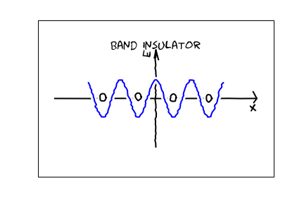
Holes
A nice cartoon of a filled band is that we put one electron of each spin state on each atom. [I just show electrons of one spin in this cartoon]
There is no conductivity, since by the Pauli principle there are no places for the electrons to go.
On the other hand, if we get rid of one electron, there is now a "hole"
When a neighboring electron "hops" into the empty space, the hole moves around. To all external appearances it looks like the conductivity is due to the motion of these "positively charged holes." [For example, in the homework you will study the "Hall effect" which measures the charge of the carriers, and indeed finds positively charged carriers in "p-type" materials."
Thus we have two types of conductors.
- n-type
- where the band is less than half full. These act like charge is being carried by negatively charged electrons.
- p-type
- where the band is more than half full. These act like charge is being carried by positively charged holes.